*Note: This page was translated by AI from the Japanese original. In case of any discrepancy, the Japanese version shall prevail.*
Overview
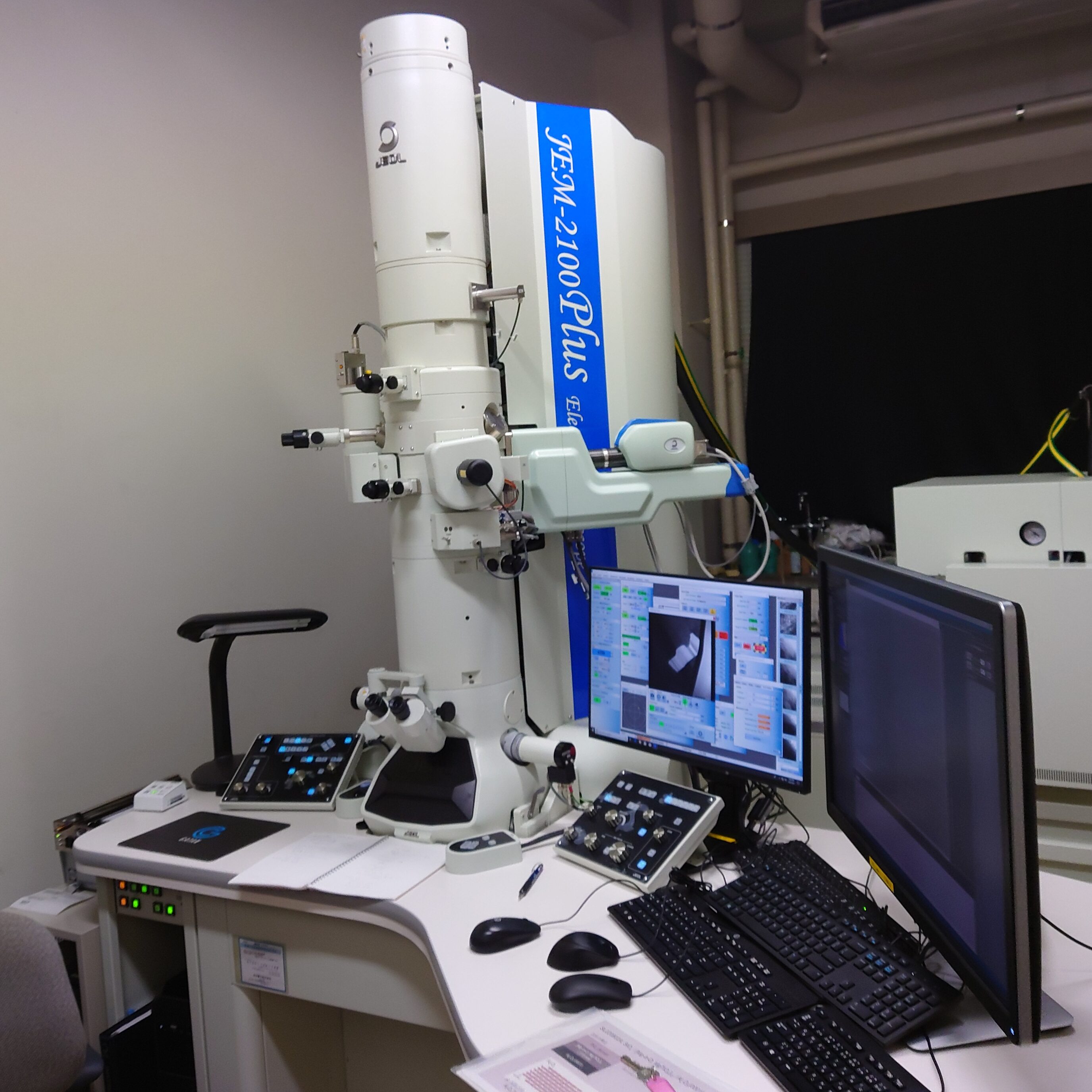
The JEOL JEM-2100Plus is a multipurpose 200 kV Transmission Electron Microscope (TEM) combining optical resolution with automated control systems.
Equipped with a cool-beam electron source and the next-generation ‘TEMCenter’ software, it performs high-resolution TEM imaging (point resolution 0.14 nm, lattice resolution 0.23 nm), electron diffraction (SAD, NBD, CBED), STEM imaging (BF/DF), and EDS microanalysis with efficiency and precision.
Features
- Next-Generation TEMCenter Interface: A compact, intuitive GUI integrating microscope control, status displays, and image viewports for automated operations.
- High-Precision Piezo-Driven Goniometer: Full computer-controlled piezo stage providing smooth sub-nanometer specimen drift stability and positioning.
- Advanced Electron Diffraction Modes: Supports Selected Area Diffraction (SAD), Nano-Beam Electron Diffraction (NBD), and Convergent Beam Electron Diffraction (CBED) for crystallographic and strain analysis.
- Digital Montage & Auto-Focus Systems: High-speed automated focusing and high-resolution panoramic montage image acquisition (equivalent to 5,000 × 5,000 pixels).
Specifications
[Specification Notice]
Actual equipment configurations or specifications may differ from standard manual specifications. Please consult the equipment manager for details regarding current capabilities and conditions of use.
Actual equipment configurations or specifications may differ from standard manual specifications. Please consult the equipment manager for details regarding current capabilities and conditions of use.
| Manufacturer | JEOL Ltd. |
|---|---|
| Model | JEM-2100Plus (Multipurpose TEM) |
| Electron Source | Cool-beam electron gun system |
| Accelerating Voltage | 200 kV (selectable: 80, 100, 120, 160, 200 kV; min step 50 V) |
| Resolution (200 kV) | Point resolution: 0.14 nm (1.4 Å) Lattice resolution: 0.23 nm (2.3 Å) |
| Magnification (MAG Mode) | ×2,000 to ×1,500,000 (LOWMAG: ×30 to ×6,000) |
| Max Specimen Tilt | X ±35° / Y ±30° |
| Analytical Capabilities | Bright-field/Dark-field TEM, STEM (BF/DF), Electron Diffraction (SAD/NBD/CBED), EDS |
| Location | Room 3-103 |