Equipment Categories
TEM/STEM
TEM sample holder
FIB/SEM
Ion Polishing
TEM sample related equipment
Electron microscope related equipment
Other devices
Software
TEM/STEM
TEM sample holder
FIB/SEM
Ion Polishing
TEM sample related equipment
Electron microscope related equipment
Other devices
Software
Equipment Categories
TEM/STEM
TEM sample holder
FIB/SEM
Ion Polishing
TEM sample related equipment
Electron microscope related equipment
Other devices
Software
TEM/STEM
TEM sample holder
FIB/SEM
Ion Polishing
TEM sample related equipment
Electron microscope related equipment
Other devices
Software
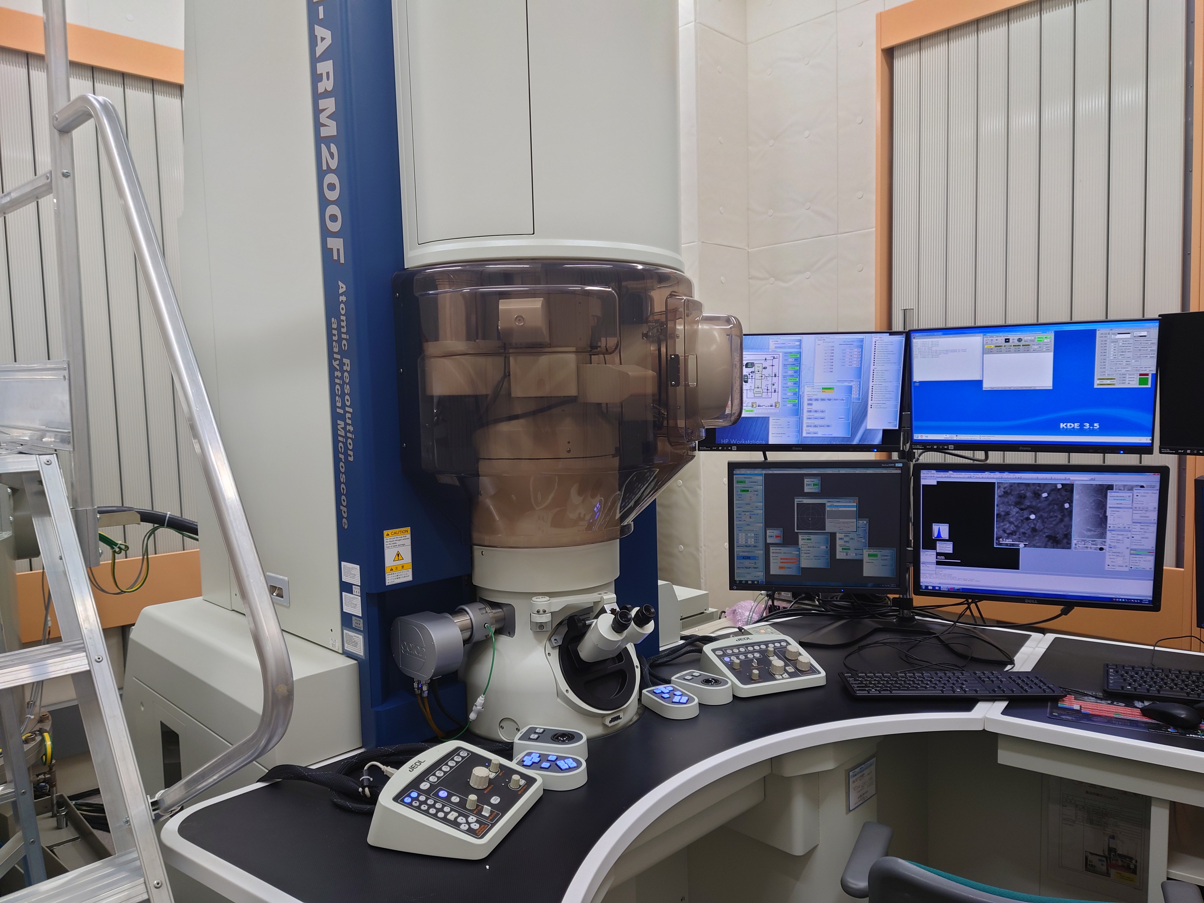
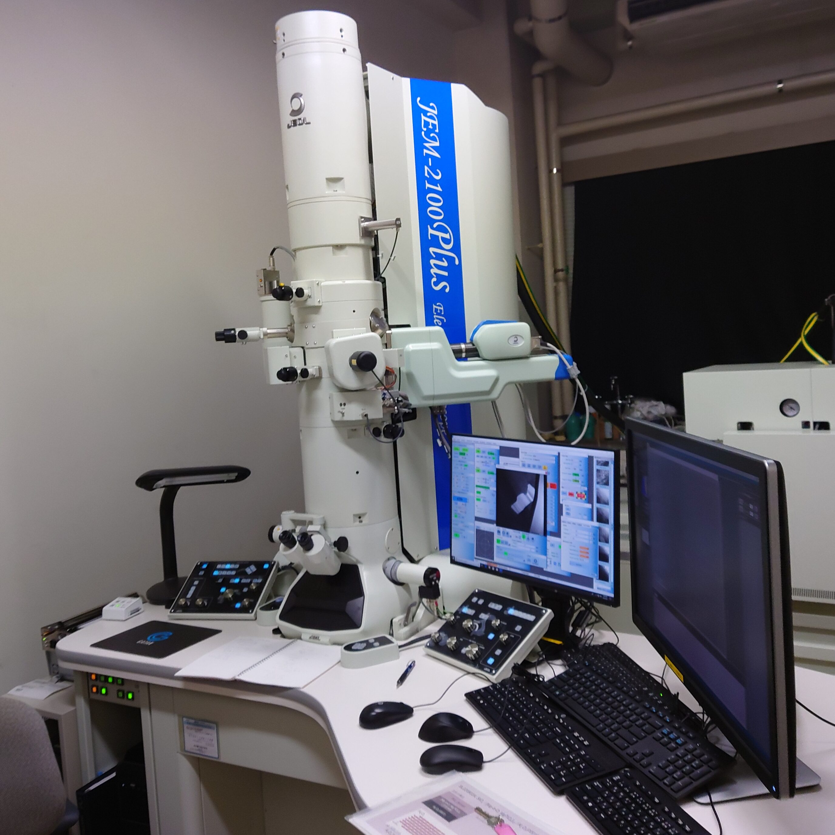
Transmission electron microscopy (TEM/STEM)
| Division | S/TEM | S/TEM | S/TEM | TEM | TEM |
|---|---|---|---|---|---|
| Appearance |  |
 |
 |
 |
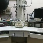 |
| Name | JEM-ARM200F W Collector |
JEM-ARM200F STEM Collector |
JEM-2100plus | EM-002B | JEM-2000EXII |
| Function | TEM/STEM/EDS/EELS | TEM /STEM/EDS/EELS | TEM/STEM/EDS | TEM/STEM/EDS | TEM |
| Location | 2-B13 | 2-B14 | 3-103 | 1-105 | 1-105 |
| Funding Source / Origin | Nanotech. Plat.*1 | Faculty of Engineering | In-house laboratory | Director’s Discretionary Fund | HVEM*2 |
| Notes | EDS malfunction High voltage malfunction up to 160kV CL fixed aperture dirty |
Slightly unstable lens |
TEM sample holder
| Classification | Sample heating holder | Sample cooling holder | Sample heating holder | Sample cooling holder | |
|---|---|---|---|---|---|
| Appearance | 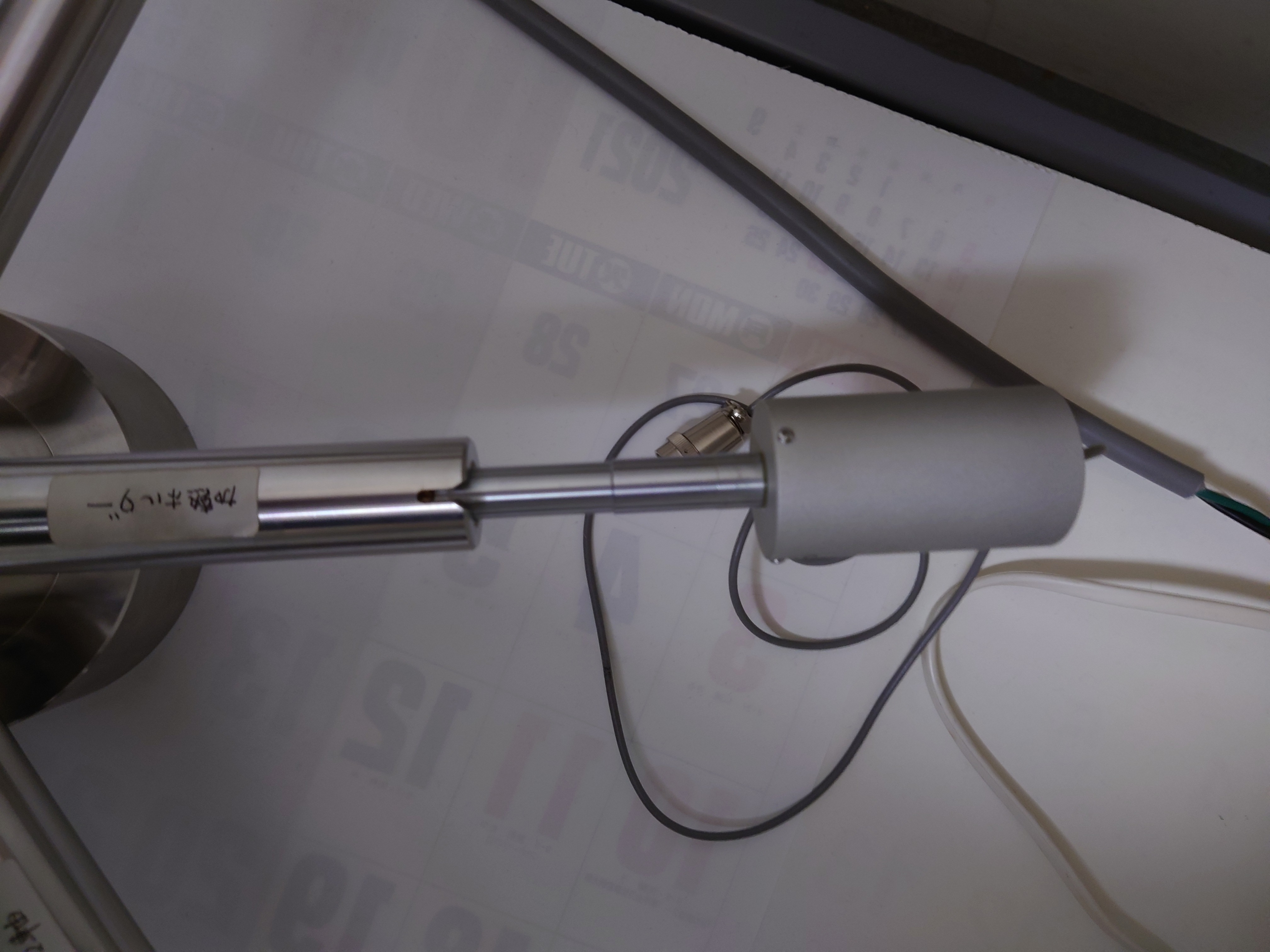 |
Photo
Coming Soon |
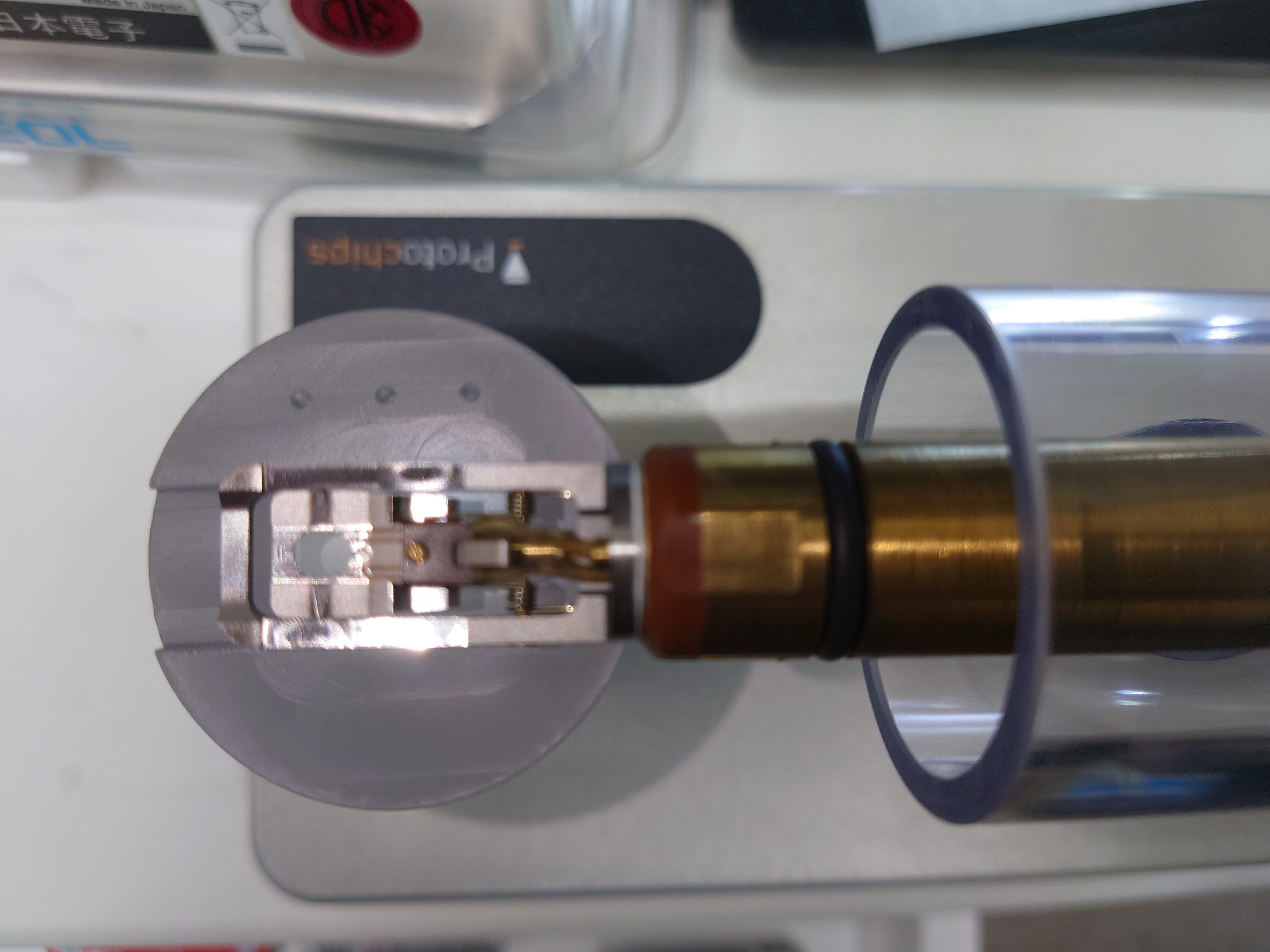 |
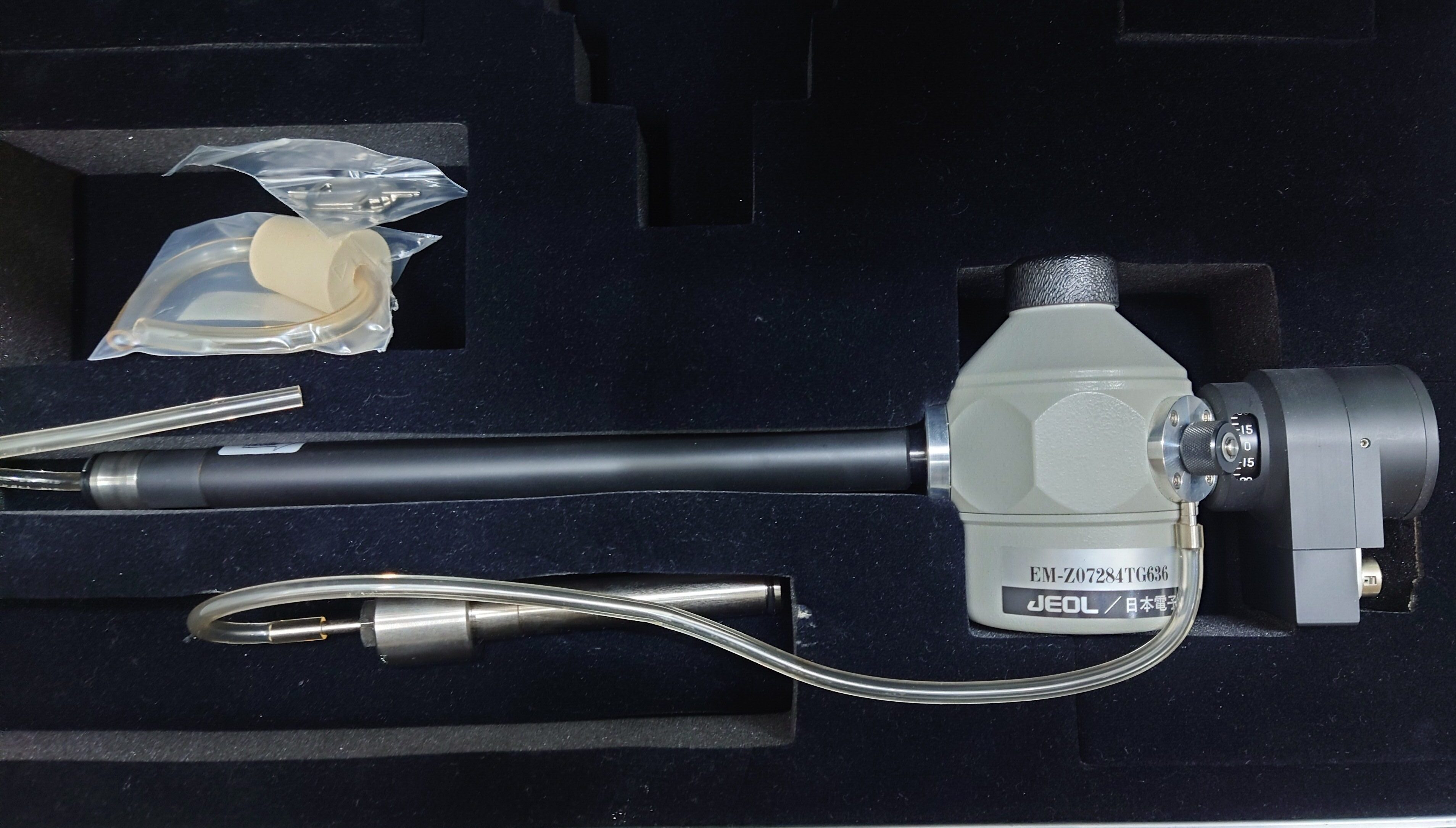 |
|
| Name | EM-SHH(4) / EM-SHTH | ||||
| Function | For JEM-2000EXII | For JEM-2000EXII | For ARM200F/2100plus Protchips |
ARM200F/2100plus For For bulk |
|
| Location | 1-105 | 1-105 | 2-B14 | 2-B14 | |
| Funding Source / Origin | HVEM*2 | HVEM*2 | Faculty of Engineering | Faculty of Engineering | |
| Notes | Adjusting | Adjusting |
| Division | Two-axis tilt holder for analysis | Reinforced specification analysis two-axis tilt holder | Single-axis tilt holder | Holder for tomography | |
|---|---|---|---|---|---|
| Appearance |
Photo
Coming Soon |
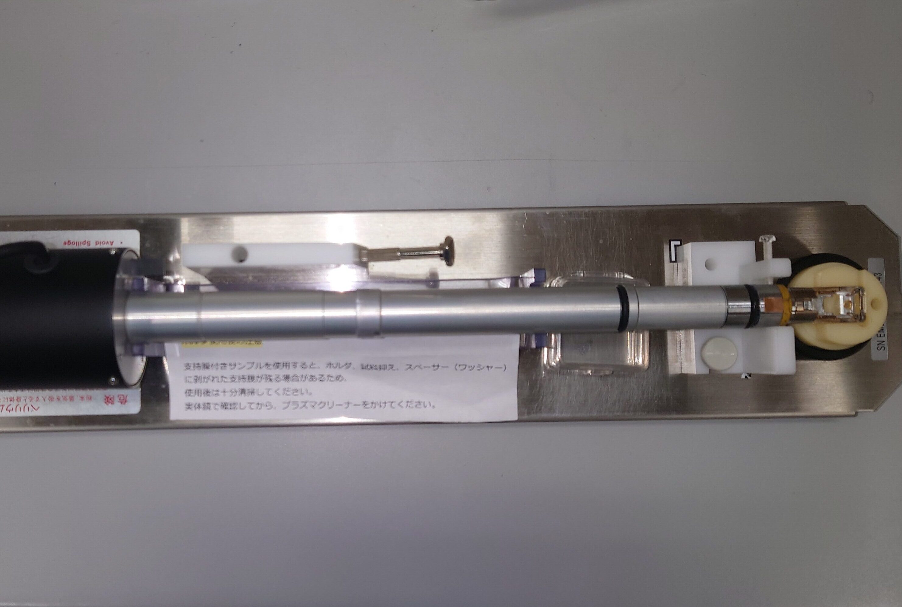 |
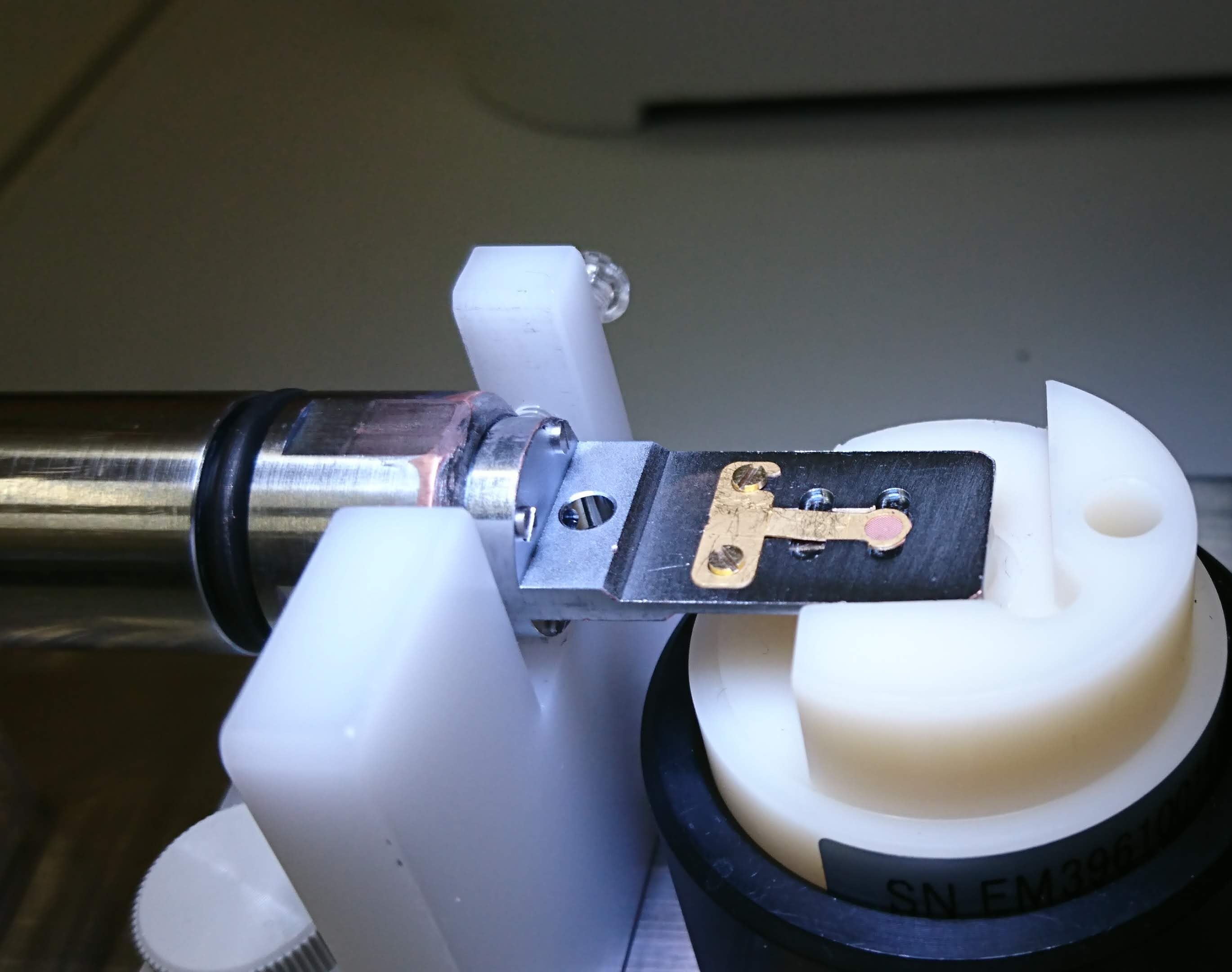 |
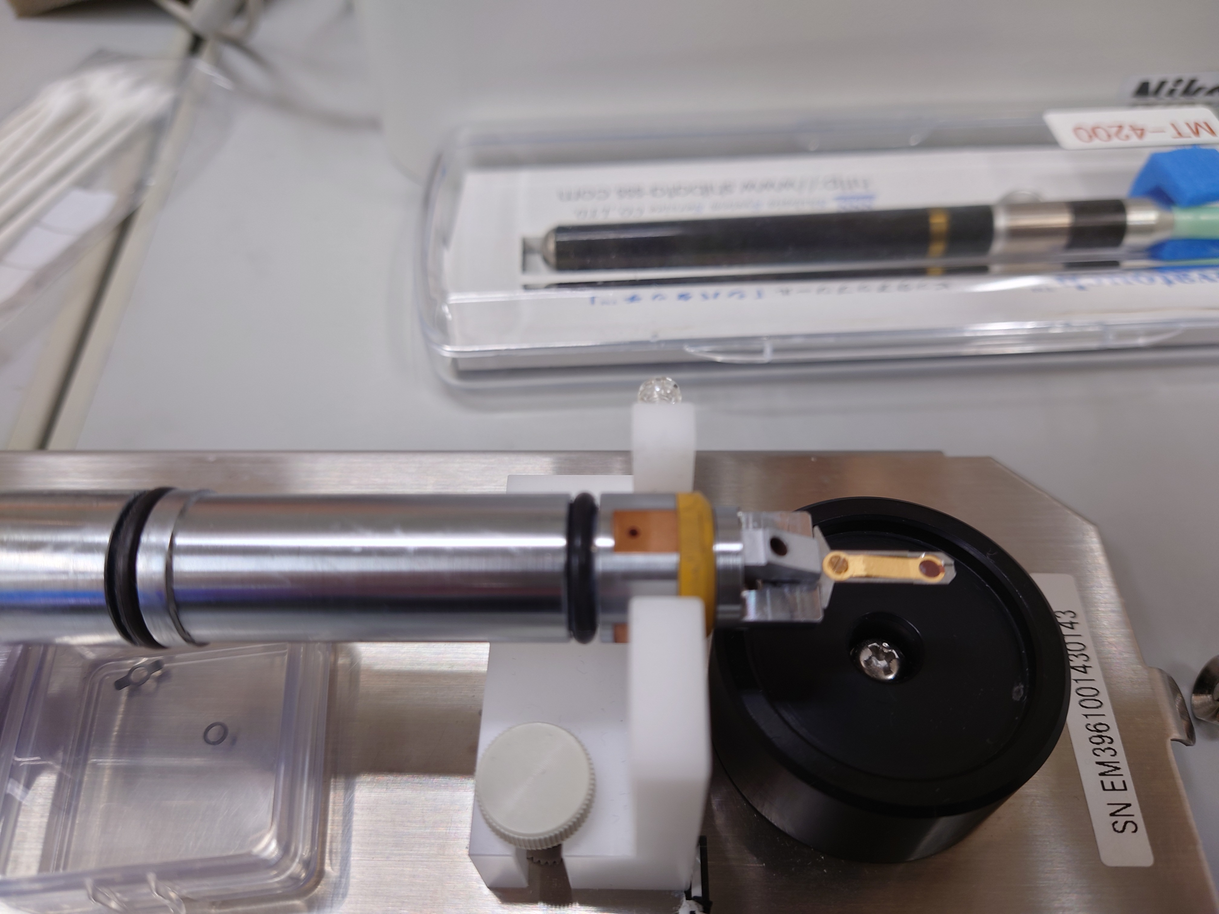 |
|
| Name | |||||
| Function | For ARM200F/2100plus | For ARM200F/2100plus | For ARM200F/2100plus | For ARM200F/2100plus | |
| Location | 3-103,2-B13 | 2-B13,2-B14 | 3-103,2-B13,2-B14 | 2-B14 | |
| Funding Source / Origin | ・HVEM*2 ・In-house laboratory |
・Nanotech. Plat.*1 ・Faculty of Engineering |
・Nanotech. Plat.*1 ・Faculty of Engineering ・In-house laboratory |
Nanotech. Plat.*1 | |
| Notes | Multiple units; origins differ | Multiple units; origins differ | Multiple units; origins differ |
FIB/SEM
| Division | FIB/SEM | FIB/SEM | FIB/SEM | ||
|---|---|---|---|---|---|
| Appearance |  |
 |
 |
||
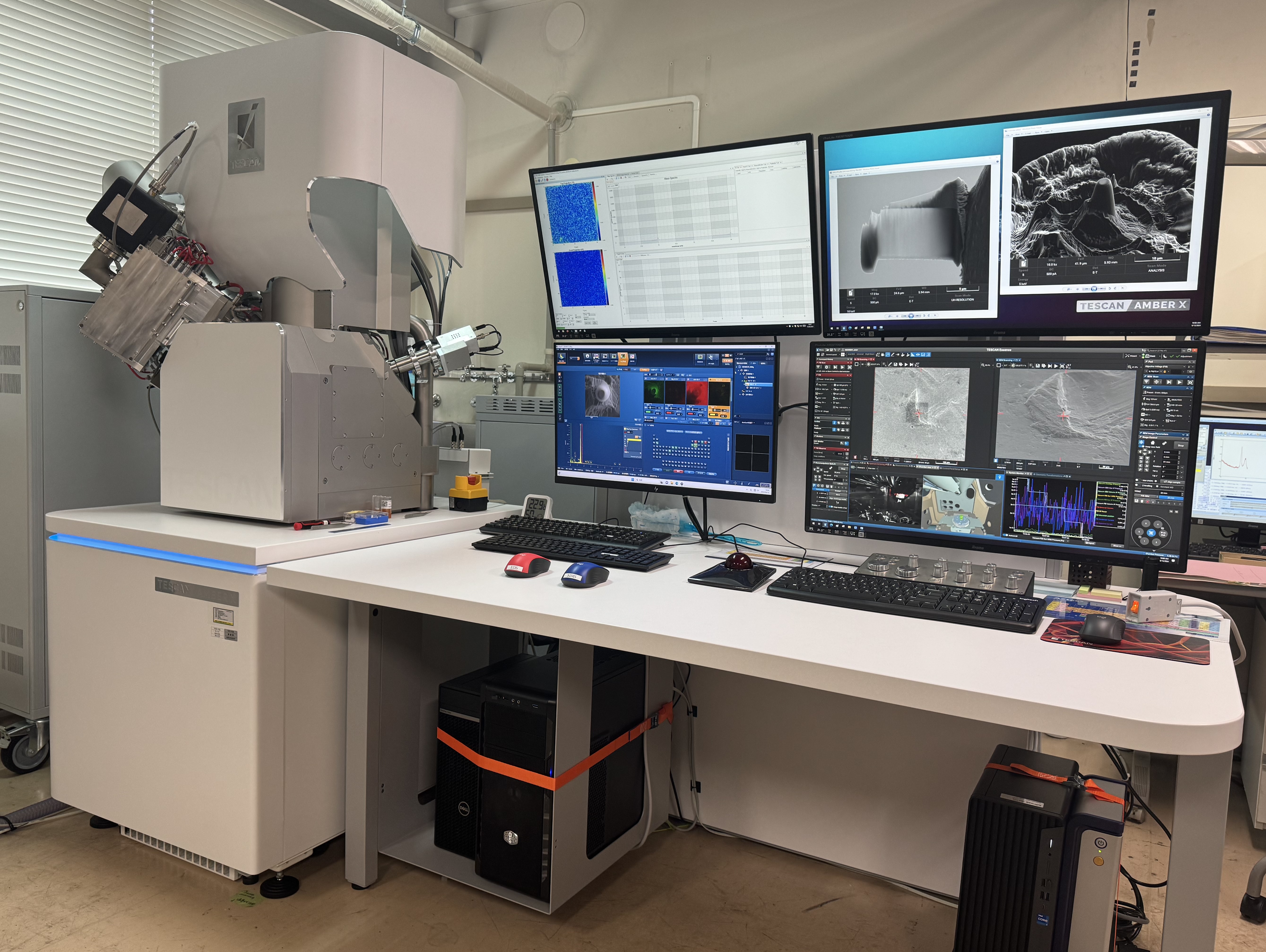
| Name | Versa 3D | Quanta 3D | AMBER X | ||
| Function | ・Dual beam Ga-FIB ・Combined SEM/FIB processing ・Micro sampling with EasyLift |
・Dual beam Ga-FIB ・Combined SEM/FIB processing ・Micro sampling with Omniprobe |
・Dual beam Xe plasma FIB ・Combined SEM/FIB processing ・TOF-SIMS capable |
||
| Location | 2-613 | 2-613 | 2 -612 | ||
| Funding Source / Origin | Nanotech. Plat.*1 | Advanced Electron Microscopy Center*2 | ARIM | ||
| Notes |
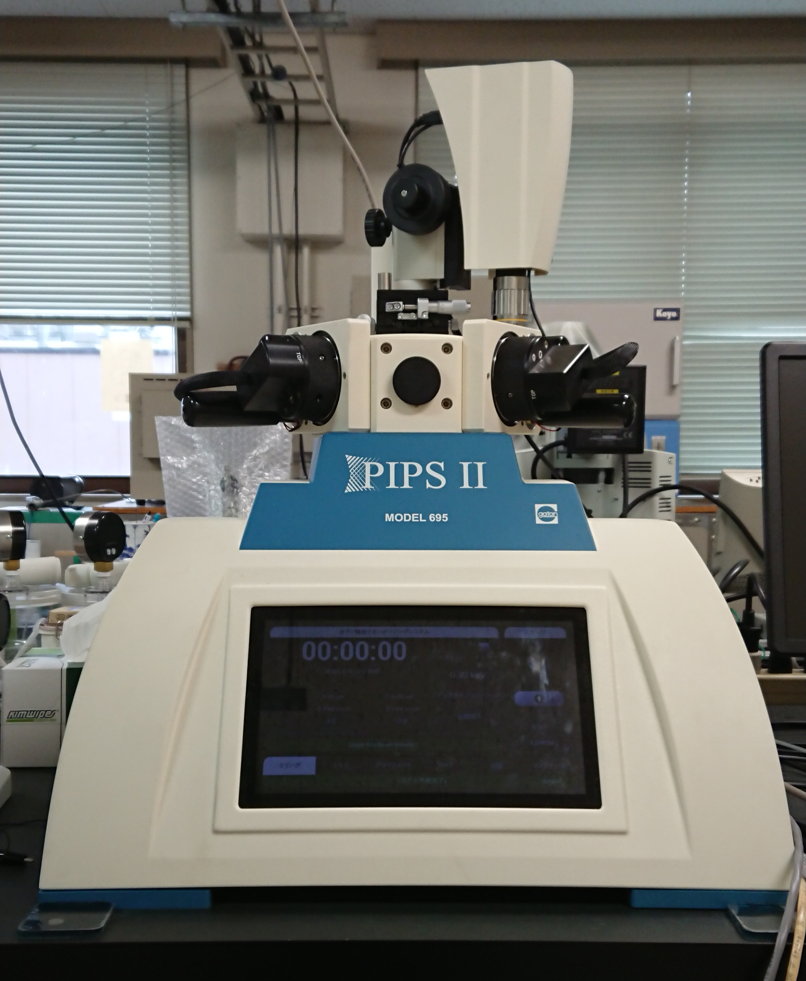
Ion Polishing
| Classification | Low-acceleration milling | Ion milling | Ion milling | Ion slicer | |
|---|---|---|---|---|---|
| Appearance | 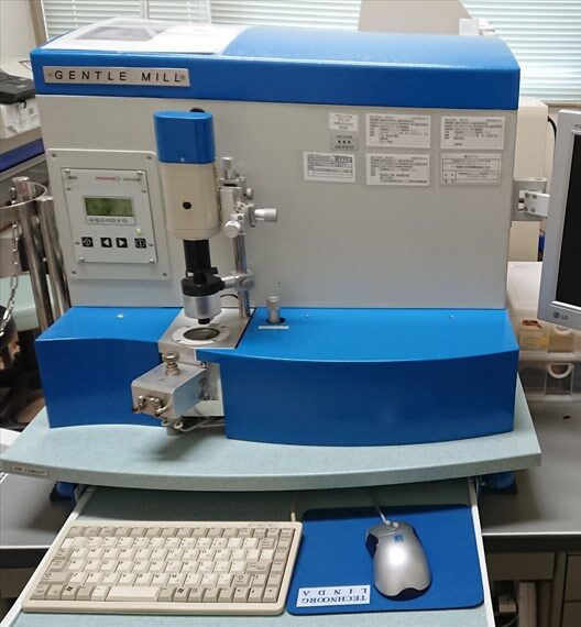 |
 |
 |
 |
|
| Name | Gentle Mill 3 | model 1010 | PIPS II(B) | EM-09100IS | |
| Function | Low energy plasma milling | Auto stop Sample cooling |
Automatic stop Sample cooling |
Cross-section sample preparation | |
| Location | 2-613 | 1-105 | 1-105 | 1-105 | |
| Funding Source / Origin | Nanotech. Plat.*1 | HVEM*2 | Nanotech. Plat.*1 | ARIM | |
| Notes | Discontinued (out of service due to failure; disposal in progress) |
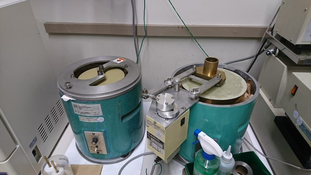
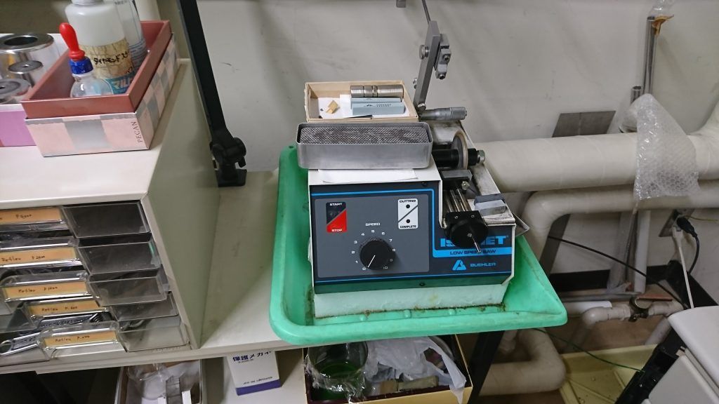
TEM sample related equipment
| Classification | Disc punch | Lap grinder | Low speed cutter | Dimple grinder | Diamond wire saw |
|---|---|---|---|---|---|
| Appearance |  |
 |
 |
 |
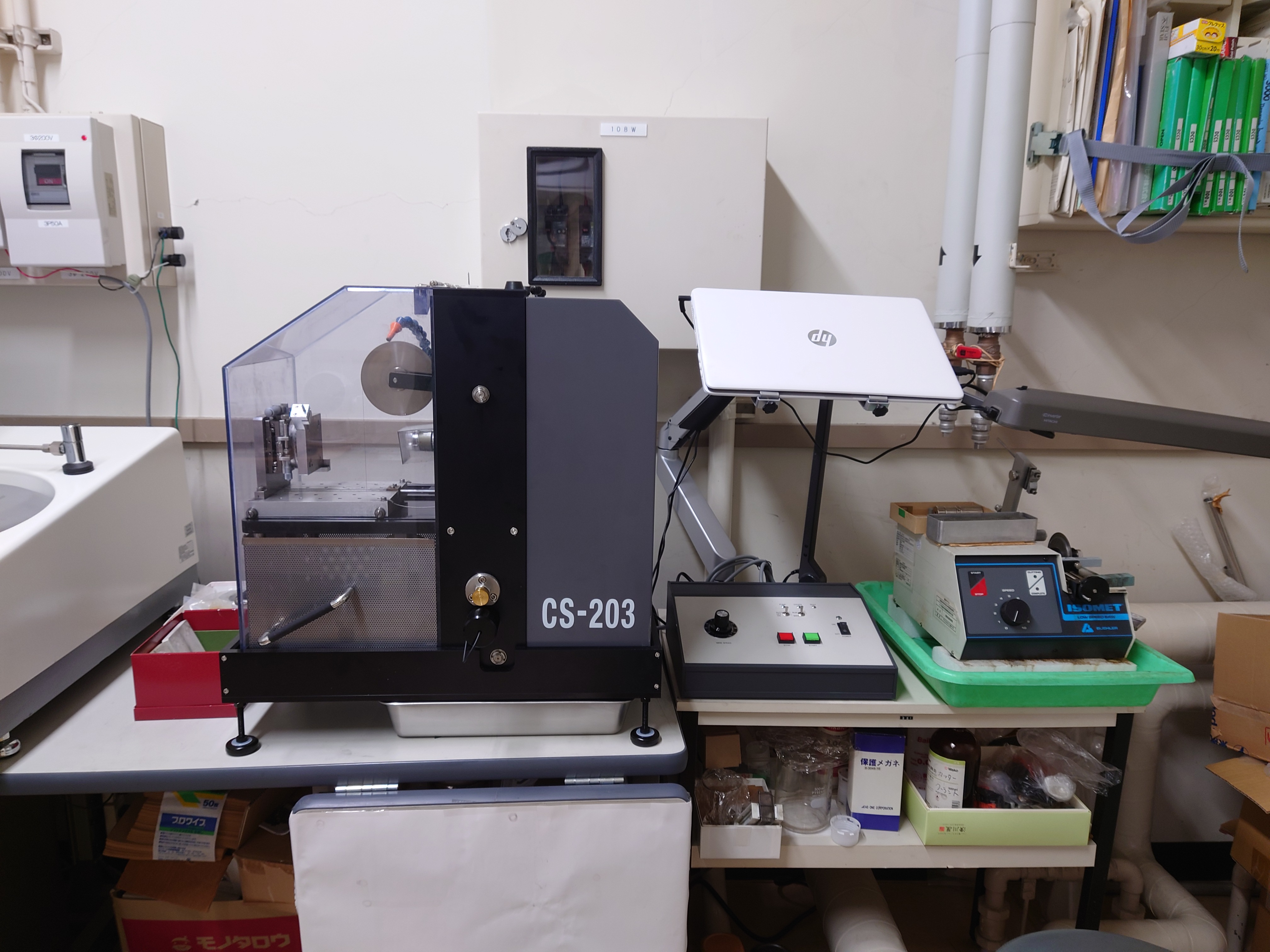 |
| Name | Homemade | Marteau | Gatan 656 | CS-203 | |
| Function | |||||
| Location | 1-105 | 1-105 | 1-105 | 1-105 | 1-105 |
| Funding Source / Origin | Advanced Electron Microscopy Center*2 | National University Reform Reinforcement Promotion Subsidy | |||
| Notes |
| Classification | Automatic polishing machine | Hot plate | Ultrasonic disc punching machine | Electrolytic polishing equipment | |
|---|---|---|---|---|---|
| Appearance | 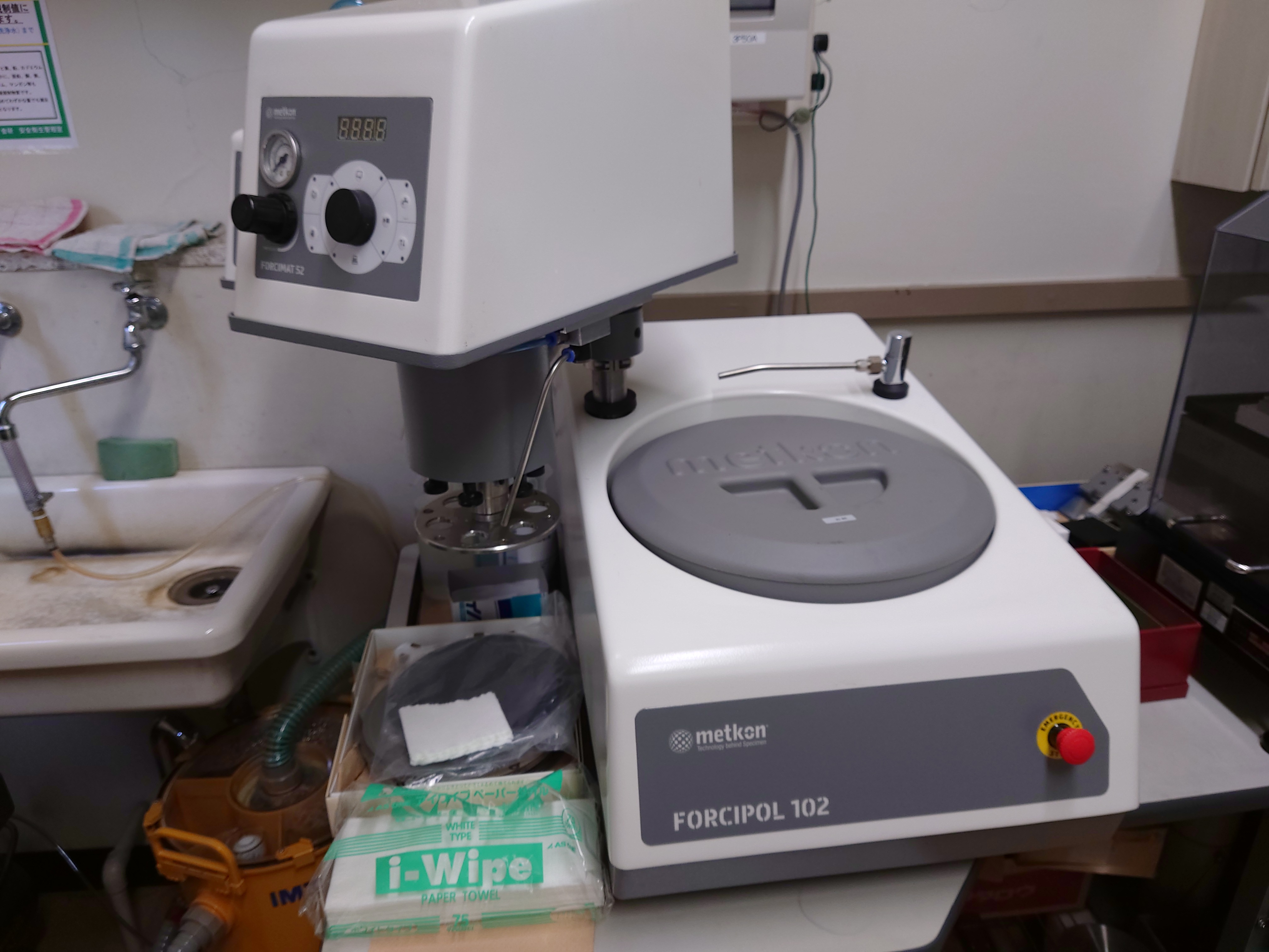 |
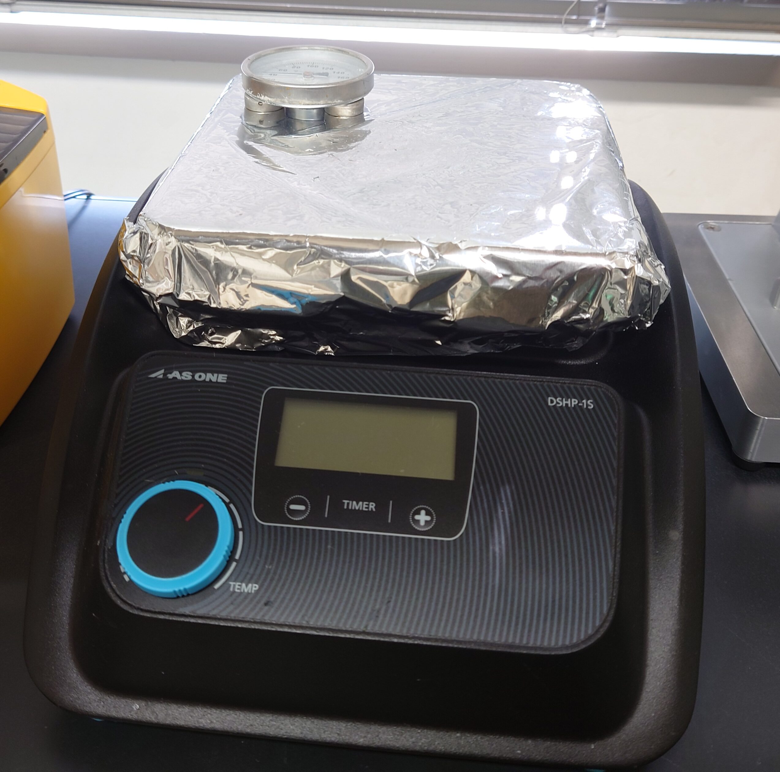 |
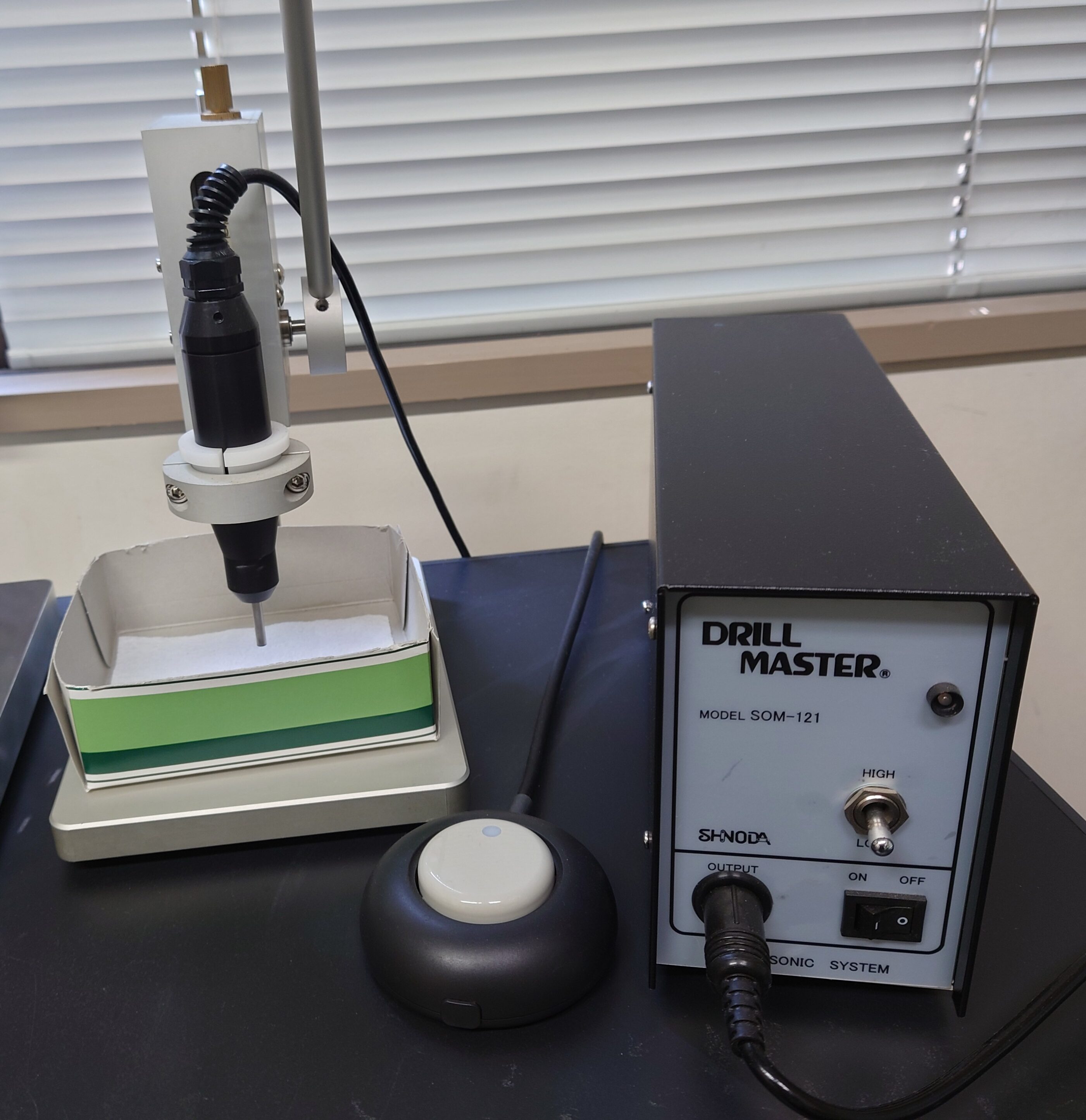 |
Photo
Coming Soon |
|
| Name | Homemade | ||||
| Features | Φ3mm disk | ||||
| Location | 1-105 | 1-105 | 1-105 | ||
| Funding Source / Origin | National University Reform Reinforcement Promotion Subsidy | In-house laboratory | |||
| Notes | Rental only |
| Division | Optical microscope | Optical microscope | Optical microscope | ||
|---|---|---|---|---|---|
| Appearance | 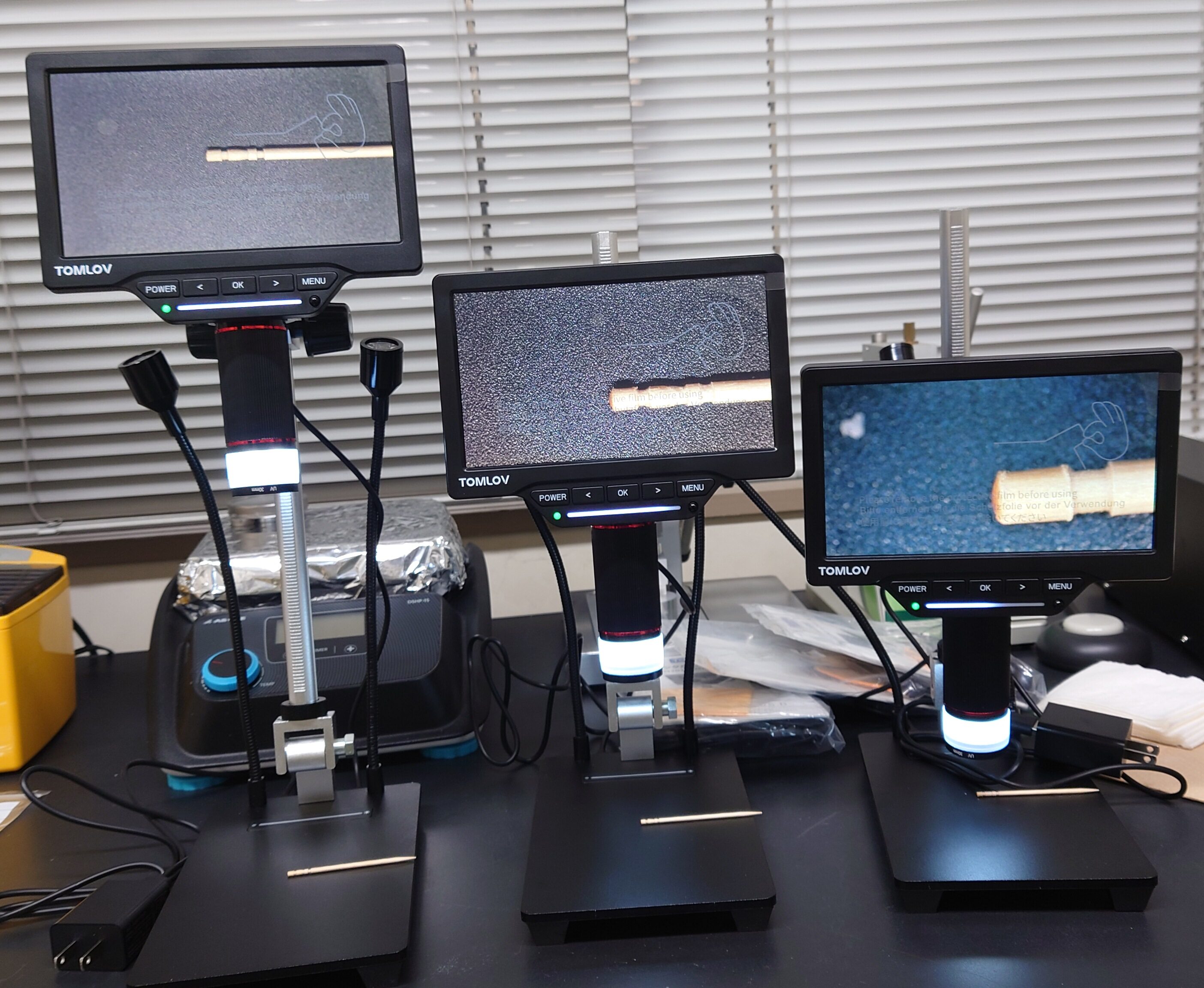 |
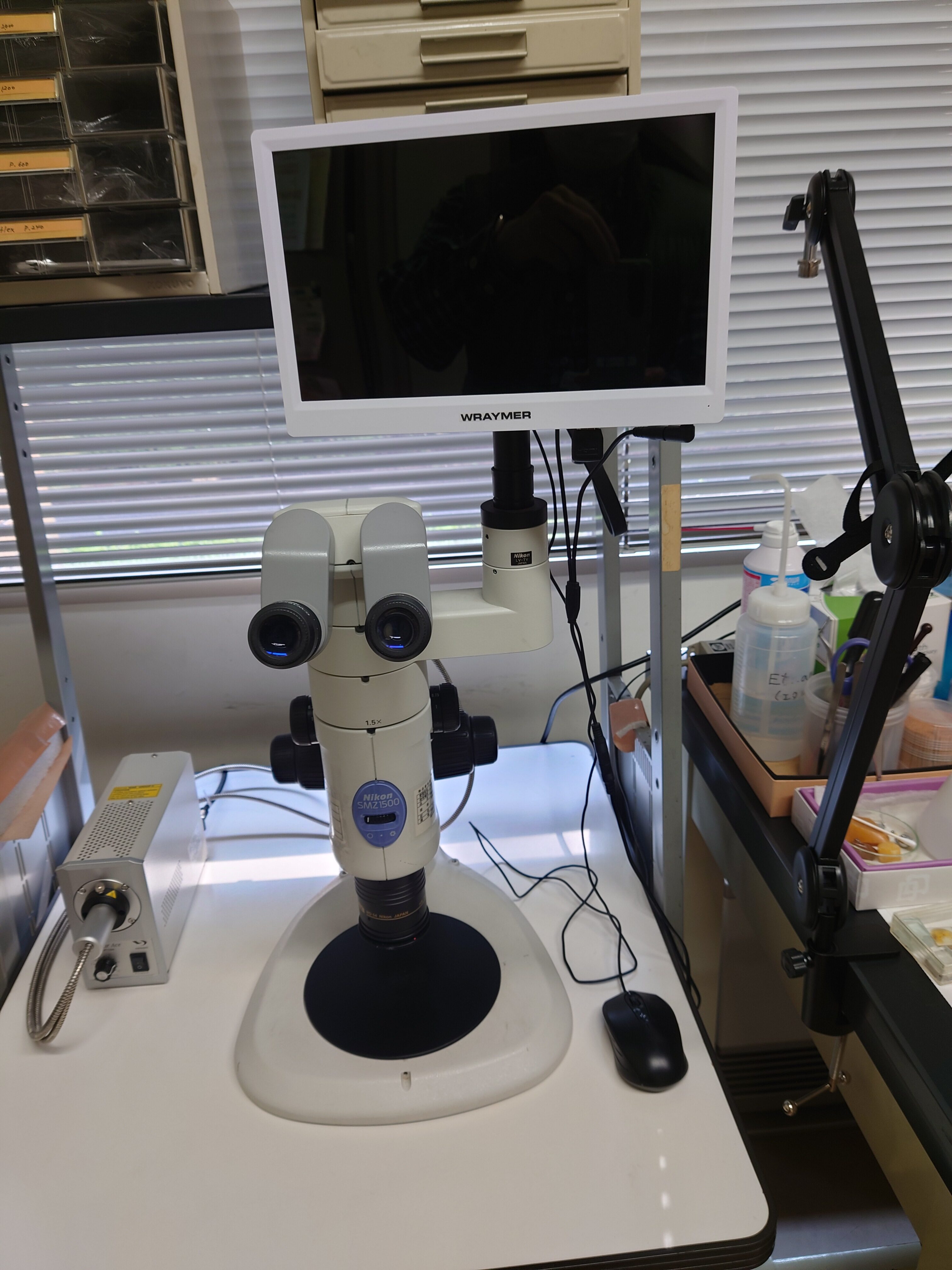 |
Photo
Coming Soon |
||
| Name | Digital microscope | Stereo microscope | Optical microscope | ||
| Features | |||||
| Location | 1-105,2-B13,2-B14,2-613,3-103 | 1-105 | 1-105 | ||
| Funding Source / Origin | |||||
| Notes |
Electron microscope related equipment
| Classification | Osmium coater | Carbon coater | Ion cleaner | Ion cleaner | Ion cleaner |
|---|---|---|---|---|---|
| Appearance |  |
Photo
Coming Soon |
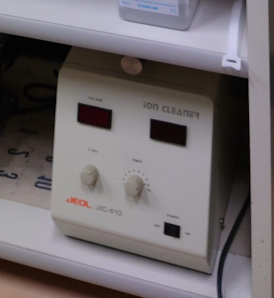 |
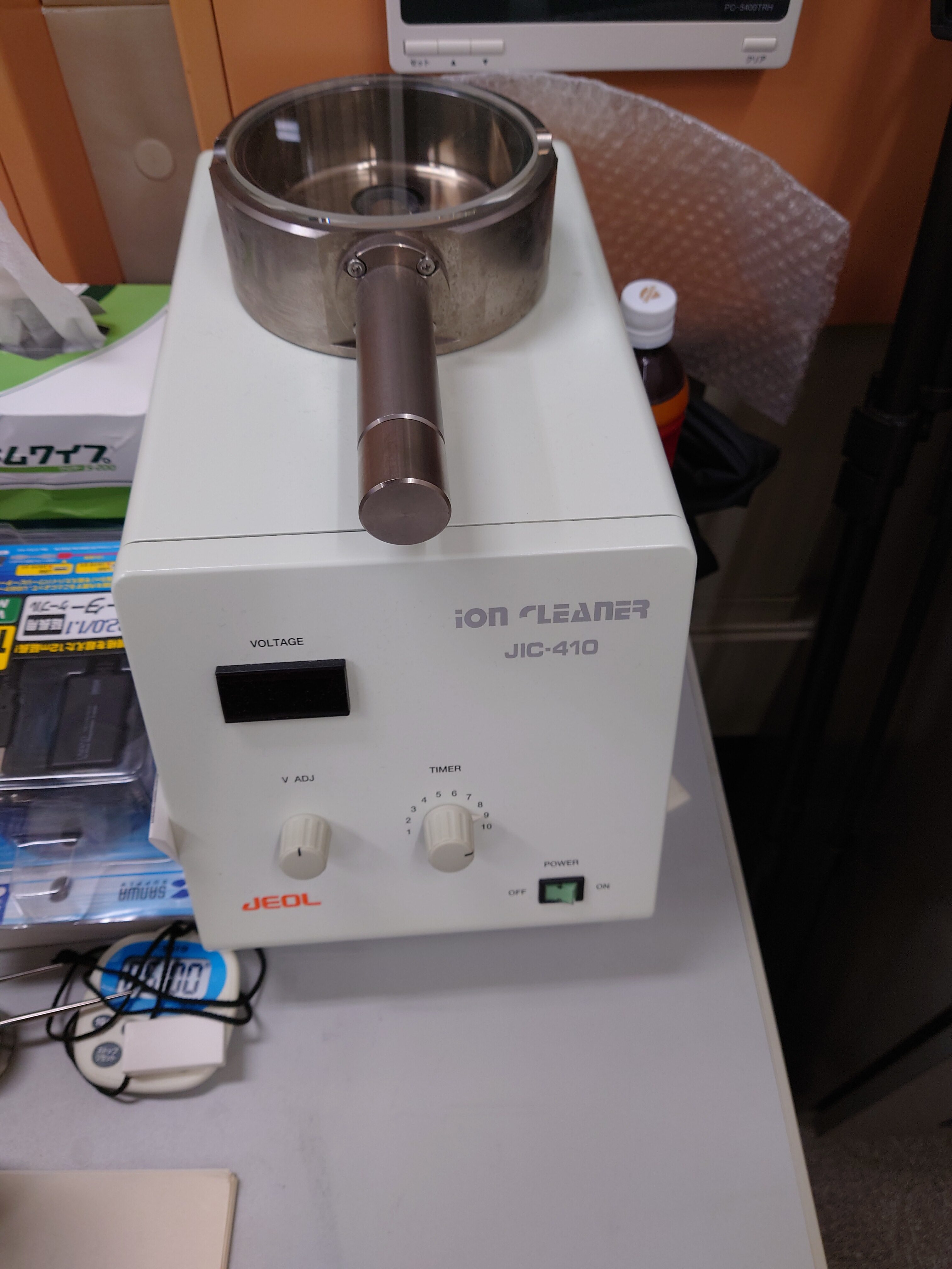 |
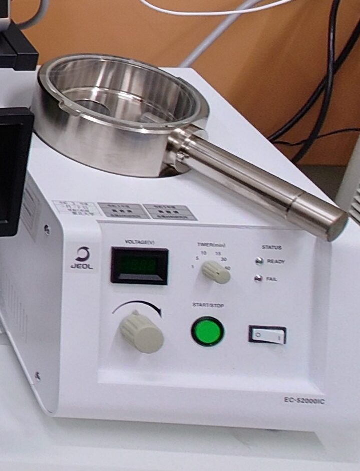 |
| Name | NEOC-PRO | ||||
| Function | |||||
| Location | 1-111 | 2-613 | 3-103 | 2-B13 | 2-B14 |
| Funding Source / Origin | Designated National University fund | Nanotech. Plat.*1 | |||
| Notes | Adjusting |
| Classification | Plasma etching equipment | Plasma cleaner | Plasma cleaner | ||
|---|---|---|---|---|---|
| Appearance |  |
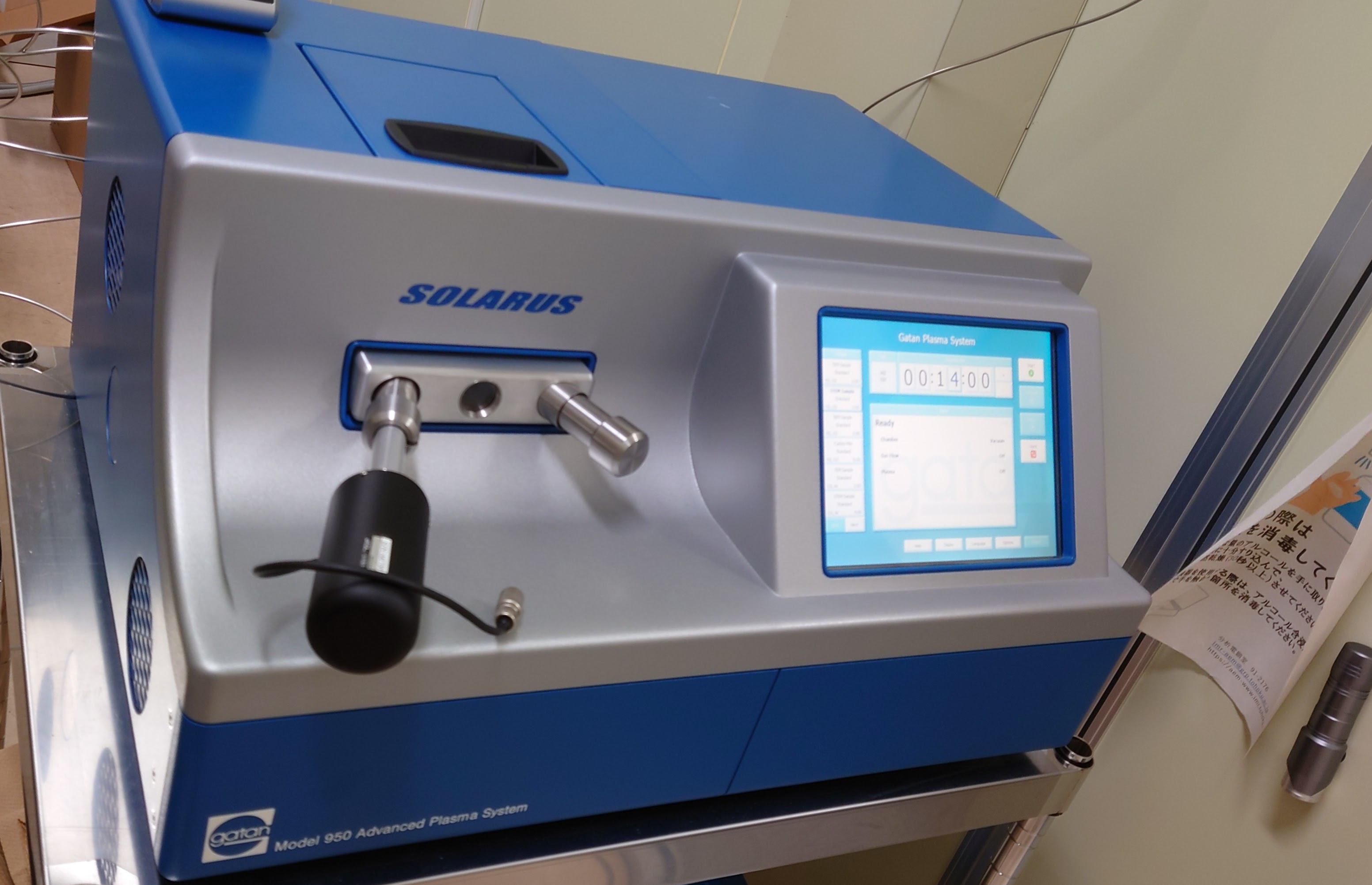 |
|
||
| Name | Solarus | Solarus | |||
| Function | Gas type: Ar,H2,O2 | Gas type: Ar,H2,O2 | |||
| Location | 1-105 | 2-B13 | 2-B14 | ||
| Funding Source / Origin | AIMR | Nanotech. Plat.*1 | |||
| Notes | Out of order/unrepairable |
Other devices
| Classification | Multipurpose X-ray diffractometer | Thermal analyzer | |||
|---|---|---|---|---|---|
| Appearance |  |
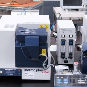 |
|||
| Name | SmartLab 9SW | Thermo plus EVO Ⅱ | |||
| Function | XRD | DSC/TG-DTA | |||
| Location | 2-613 | 2-613 | |||
| Funding Source / Origin | Nanotech. Plat. Molecular Synthesis PF*1 | Nanotech. Plat. Molecular Synthesis PF*1 | |||
| Notes |
Software
- Crystal structure modeling/electron diffraction simulation
- High-resolution electron microscope image simulation
Note: The "Funding Source / Origin" column shows the name of the organization at the time the equipment was transferred to our division.
*1 Nanotech. Plat. = Nanotechnology Platform, formerly a MEXT/JST shared-facility program; currently named ARIM (Advanced Research Infrastructure for Materials and Nanotechnology).
*2 HVEM = the High-Voltage Electron Microscope Laboratory; currently named TCEM (Tohoku Center for Electron Microscopy).
Note: A blank "Funding Source / Origin" cell may indicate a low-cost purchase (not separately recorded) or an origin that is currently unknown.
This page was created by an AI agent.